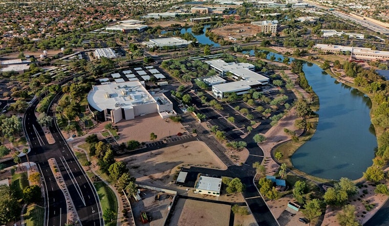
The Biden-Harris administration, together with the Department of Commerce and Natcast, have identified the Arizona State University (ASU) Research Park in Tempe, Arizona as the planned site for the third flagship CHIPS for America research and development (R&D) facility. This new endeavor is poised to fuel semiconductor innovation, with the facility expected to become operational in 2028. In a statement obtained by the Department of Commerce, U.S. Secretary of Commerce Gina Raimondo highlighted the importance of R&D, saying, "A strong research and development ecosystem is essential to ensuring the United States remains at the forefront of semiconductor innovation."
The chosen site falls within an area already known for its tech advancements. Carrying the agenda of the bipartisan CHIPS and Science Act, the facility aims to cultivate a more robust domestic supply chain and reinforce U.S. standing in a critical sector that intertwines with both economic growth and national security. Set to foster the development and testing of new semiconductor materials and devices, the facility will bridge the gap between research in our laboratories and the commercial production floor, announced White House Deputy Chief of Staff Natalie Quillian, according to the same press release.
Presently, a key challenge within the semiconductor industry does the transition from scaling new technologies in research to robust production. The forthcoming CHIPS for America facility endeavors to address this by offering integrated R&D activities and prototyping capabilities, including at least one 300mm full-flow complementary metal-oxide-semiconductor (CMOS) technology. Moreover, the Advanced Packaging Piloting Facility will enable experiments in a controlled, manufacturing-like environment, which is not viable in actual production sites.
Spanning across academia and industry, partnerships formed because of this facility are set to unleash a flurry of opportunities for collaborative, hands-on research utilizing cutting-edge tools and equipment essential for workforce development. Natcast CEO Deirdre Hanford conveyed this sentiment, telling the Department of Commerce, “This facility will be a premier destination where researchers from industry, academia, startups, and the broader semiconductor ecosystem will convene to explore, experiment, and collaborate on the next generation of semiconductor and packaging technologies that will power the industries of the future.”
The integration of the PPF with Arizona's burgeoning microelectronics sector and the vibrant research activities at ASU heralds a synergistic approach that could lead to substantial advances in semiconductor R&D. Alongside the EUV Accelerator and the Design and Collaboration Facility, these flagship R&D centers are purposed to craft world-class destinations for semiconductor innovation in the U.S. They will serve a wide-ranging community including universities, small businesses, large manufacturers, and government agencies. These interconnected institutions vow not only to bolster cutting-edge research but also to generate new job prospects, representing an emblematic stride forward in reinvigorating American industrial prowess. More details on this partnership and associated technical centers are expected to be unveiled in the coming months by the Department of Commerce and Natcast.


