Syenta, an Australian semiconductor startup, has picked Tempe for its first beachhead in the United States, opening a 3,500-square-foot demonstration and development lab at Arizona State University's Research Park on Tuesday, April 21, 2026. The site, which the company says will support roughly 200 high-skilled roles, is built around prototype tools and testing rigs for advanced chip packaging meant to speed the journey from lab to customer for next-generation AI chips. Local officials say the move plugs the Australian National University spinout directly into the Valley's fast-growing semiconductor ecosystem.
According to the Arizona Commerce Authority, the ASU Research Park facility is expected to support about 200 positions in semiconductor engineering, systems architecture and advanced manufacturing. The agency describes the Tempe site as a demonstration and partner-engagement hub for Syenta's Localized Electrochemical Manufacturing (LEM) platform.
“Tempe is a natural choice for our first U.S. operations,” Syenta CEO Jekaterina Viktorova said in the announcement via the Arizona Commerce Authority. The release adds that co-locating at ASU Research Park will let Syenta “leverage faculty expertise and state-of-the-art facilities” as it works with American chipmakers and investors.
What Syenta Builds
Syenta's Localized Electrochemical Manufacturing (LEM) is described as a high-resolution metallization process designed to create denser chip-to-chip interconnects, which can improve memory bandwidth for AI systems. The Tempe expansion follows a Series A1 financing and backing that includes an A$10.1 million investment from Australia's National Reconstruction Fund as part of a roughly US$26 million round to scale production and U.S. engagement, according to the NRFC.
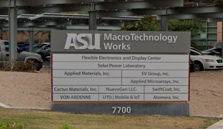
Why Tempe
Economic-development groups said Tempe's Research Park, with direct ties to ASU talent and nearby packaging and prototyping projects, made the city a logical first U.S. stop for the company. The Greater Phoenix Economic Council noted that the move strengthens the region's semiconductor ecosystem, and Axios Phoenix reports ASU was selected as one of the CHIPS R&D facility sites that further anchor advanced packaging work in the Valley.
Jobs and Hiring
Syenta said it is actively hiring for process and applications engineering roles and pointed jobseekers to its careers pages as it starts operations in Tempe, per Syenta. Local leaders stressed that the emphasis will be on high-skilled engineering and prototype-manufacturing positions rather than large-scale factory hires.
The Tempe lab joins a flurry of Valley semiconductor activity, from TSMC's north Phoenix projects to Amkor's packaging investments, and officials say Syenta's footprint helps broaden the area's prototype-to-production pipeline. For more information, see Syenta's announcement and the Arizona Commerce Authority's statement linked above.