Engineers from MIT have made a breakthrough in materials science, creating a complete map for elastic strain engineering, a technique that can fine-tune material properties for a variety of applications, according to MIT News. The team, led by Ju Li, the Battelle Energy Alliance Professor in Nuclear Engineering and professor of materials science and engineering, employed advanced machine learning algorithms and first principles calculations to achieve this feat, which has broad implications for the semiconductor industry and other technology sectors.
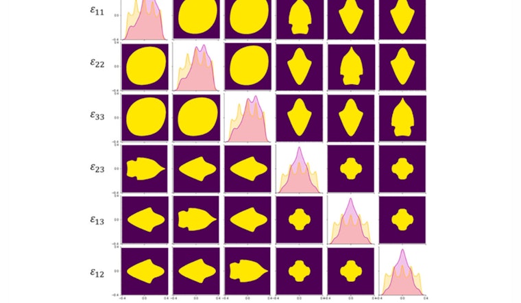
The development of this map is a milestone in the understanding of how materials behave at the micro- and nano-scales with previous assumptions often falling short at these tiny dimensions, it's long been known that properties of bulk materials don't always apply when shrunk down. Li told MIT News, "For the first time, by using machine learning, we’ve been able to delineate the complete six-dimensional boundary of ideal strength, which is the upper limit to elastic strain engineering." This new method surpasses traditional methods of creating new materials that usually involved altering chemical compositions.
Elastic strain engineering involves applying controlled strains to a material to alter its thermal and electronic properties without causing permanent deformation or damage. This technology can potentially revolutionize the performance of semiconductors by adjusting diamond nanoneedles, for instance, to endure strains up to 9 percent and still return to their original form. Such capabilities were previously demonstrated by Subra Suresh, the Vannevar Bush Professor of Engineering Emeritus, and colleagues.
Armed with their pioneering map, MIT researchers are looking at a multitude of exotic material properties, such as significantly improved thermal conductivity and possibly even superconductivity, Li suggested that strain engineering could even improve diamond's thermal conductivity by a factor of two, conversely it could make it much worse by a factor of 20 depending on how the strain is applied, which has profound implications for the design and efficiency of future electronic devices, according to MIT News. Zhe Shi, a postdoc in Li's lab and first author of the paper, acknowledged that while the research is promising, there is a considerable amount of manufacturing and device issues that need addressing before these findings are routinely applied in consumer technology.
This groundbreaking work was underpinned with support from various funding sources including the Defense Threat Reduction Agency, an NSF Graduate Research Fellowship, and the National Science Foundation (NSF). The innovative study points to a new era of materials design where elastic strain rather than chemical alteration takes center stage, potentially leading to advancements in the speed and performance of not just microchips, but a broad spectrum of devices in the tech industry.