In a notable advancement for the electronics industry, MIT researchers, along with their international partners, have crafted a novel method for integrating two-dimensional materials into electronic devices without damaging them. This breakthrough, as explained in MIT News, could pave the way for the development of superior computers and other high-performance devices with enhanced electrical and optical properties.
Two-dimensional materials have long tantalized scientists with their ability to conduct electricity with exceptional efficiency, but the challenge has been incorporating them into hardware due to their delicate nature. Traditional manufacturing techniques, relying on aggressive chemicals and high temperatures, tended to wreak havoc on these atom-thin layers. However, the new technique developed by researchers sidesteps these issues by employing a single-step process that keeps the integrity of the 2D material intact, according to a paper published in Nature Electronics.
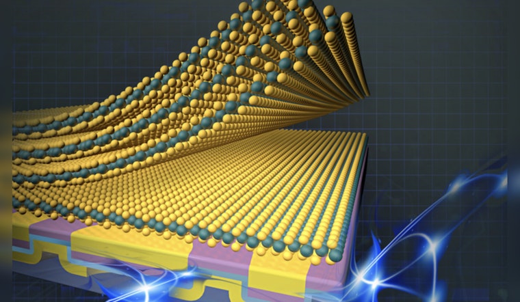
The method utilizes van der Waals forces—natural attractions present between all matter—to stick the 2D materials onto device layers that have already been created. In a statement obtained by MIT News, Farnaz Niroui, assistant professor of electrical engineering and computer science at MIT and senior author of the study, elucidated that "Since these forces depend on the intrinsic properties of the materials, they cannot be readily tuned." The innovation her team has introduced addresses this limitation, enabling traditionally incompatible materials to be fused together, bringing forth devices with new and potentially groundbreaking functionalities.
With this technique, the researchers have overcome the limitation of van der Waals forces by embedding a low-adhesion insulator within a high-adhesion matrix, making it possible to attach 2D materials to surfaces where they wouldn't naturally adhere. For instance, the team successfully fabricated p-type transistors—generally challenging to produce with 2D materials—featuring improved functionalities over previous methods. Peter Satterthwaite, an electrical engineering and computer science graduate student and lead author of the study, described how the "hybrid surface is brought into contact with the 2D layer without needing any high temperatures, solvents, or sacrificial layers," hence enabling the formation of fully functional devices efficiently.
The prospects this new platform presents are vast, ranging from high-performance computing to flexible electronics. The MIT-led team aims to further explore this technique to integrate a wider variety of 2D materials, studying their inherent properties unimpeded by process-related damages. The potential to revolutionize the way electronic devices are built, potentially leading to faster, more efficient, and possibly even more environmentally friendly gadgets, has significant implications for future technologies. This research received partial funding from prestigious U.S. institutions, including the National Science Foundation and the Department of Energy, highlighting its significance in the scientific and technological community.