Union City just scored a serious upgrade in the tech world. Japanese materials firm Resonac has opened what industry and company announcements describe as the first U.S. research center dedicated to advanced semiconductor packaging, planting a key piece of the AI supply chain in this East Bay city.
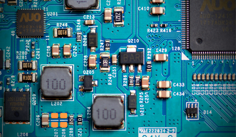
The new R&D hub zeroes in on the often overlooked stage where bare silicon wafers are transformed into stacked, high-performance modules that power AI servers, data center hardware, and smartphones. City officials say the facility is expected to bring new jobs and tighter technical ties between Silicon Valley chip customers and Japanese suppliers, while putting Union City on the map in a field usually dominated by larger tech hubs.
In a company announcement, Resonac said the Union City site will house US-JOINT, a co-investment consortium of about a dozen U.S. and Japanese materials and equipment companies, and will feature cleanrooms and evaluation tools designed to speed proof-of-concept work, according to a press release from Resonac. The goal is to let participating firms test and validate new packaging ideas side by side with major chip customers in nearby Silicon Valley. The opening caps several years of planning and buildout for what Resonac describes as its Silicon Valley base.
Resonac president and CEO Hidehito Takahashi called the launch “a milestone in industry” and said the company wanted to be physically close to the big cloud companies that buy cutting-edge chips. “Silicon Valley has this unique atmosphere of fast-paced work compared to, let's say, Japan, which is a little slower,” Takahashi told ABC7. Company officials say the proximity should shorten proof-of-concept cycles and help promising ideas reach commercialization faster.
Who’s involved
The US-JOINT consortium pulls together a mix of equipment makers and materials suppliers, including KLA, Kulicke & Soffa, 3M and Toppan. The Union City center will run class-100 and class-1,000 cleanrooms for evaluation and development work, according to an announcement from ULVAC. The facility is pitched as a place where fabless chip designers, semiconductor manufacturers and equipment engineers can quickly validate new packaging techniques without having to leave the United States.
Why packaging matters
Advanced packaging, which includes stacking chips, using interposers and other steps that come after wafer fabrication, has become a critical chokepoint for U.S. chip supply chains as demand for AI silicon explodes. The U.S. Department of Commerce has steered funding toward building domestic capacity in this area, and the CHIPS National Advanced Packaging Manufacturing Program recently finalized roughly 1.4 billion dollars in awards to support advanced packaging research and pilot runs, according to a Commerce bulletin. Industry analysts say private R&D hubs like the new Union City center are meant to complement those federal investments by helping promising ideas move from the lab to pilot production.
“We hope it's not only going to benefit the customer and the companies that use those chips but it's also going to bring more jobs to Silicon Valley and to Union City,” Gloria Ortega, the city's economic development manager, told ABC7. Officials did not immediately release a jobs estimate, but said the center will start with a small R&D team and visiting engineers from consortium partners. Local leaders say they are betting that the project will raise Union City's profile among global technology investors.
Industry outlets have pointed to the inauguration as evidence that U.S. co-creation models for chip packaging can work, and say the Union City site gives the region a foothold in the global race to advance semiconductor technology, according to Silicon Semiconductor. Consortium members say they expect development timelines to shrink from months to weeks by enabling face-to-face collaboration with major customers.
For Union City, long seen as a modest industrial community on the East Bay, the Resonac center is both a symbolic victory and a real-world test of whether it can host cutting-edge chip work. Partners are expected to roll out more announcements in the coming months as projects move from early validation to pilot production and, potentially, to local hiring on a larger scale.