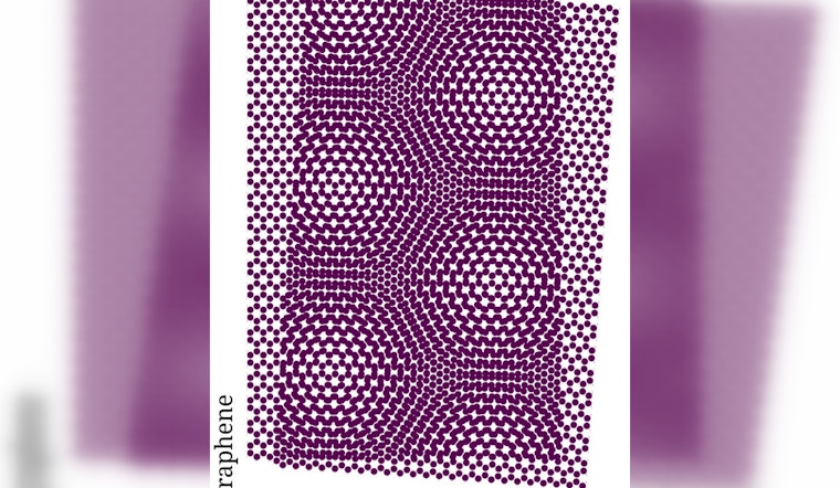
The ever-evolving domain of condensed-matter physics is gaining accelerated momentum, thanks to the innovative work of Harvard scientists who have recently introduced a more efficient method for exploring twistronics, specifically concerning the twisting of ultra-thin materials. Twistronics, a field that investigates the electrical properties of materials like graphene when layers are twisted at specific angles, has seen significant advancements due to a new machine capable of manipulating these angles with greater ease than ever before.
Researchers at Harvard, among them physicists Amir Yacoby and Eric Mazur, have refined the groundwork laid by Yuan Cao's 2018 breakthrough in magic-angle graphene superlattices. They have shared details about a fingernail-sized machine in a paper published in Nature, which can twist thin materials on-demand, a marked improvement over the previously labor-intensive process. This micro-electromechanical system-based actuation platform, or MEGA2D, has the potential to usher in a host of discoveries with applications ranging from transistors to quantum computers.
"Controlling density has been the primary knob for discovering new phases of matter in low-dimensional matter, and now, we can control both density and twist angle, opening endless possibilities for discovery," Yacoby said in a statement obtained by the Harvard Gazette. The ease of use this groundbreaking technology introduces cannot be overstated; it simplifies the previously arduous process of fabricating twisted devices one by one.
Assistant Professor Yuan Cao, a frontrunner in the development of twisted bilayer graphene and a key player in the twistronics frontier, commended the MEGA2D platform for its potential to solve complex puzzles in the field. Cao told the Harvard Gazette, "By having this new 'knob' via our MEGA2D technology, we envision that many underlying puzzles in twisted graphene and other materials could be resolved in a breeze." Enthusiasm for the new device reaches well beyond its creators, as it promises to be a boon to researchers across the globe.
Demonstrating the MEGA2D device's broad utility, the Harvard team successfully applied it to hexagonal boron nitride, shedding light on the technological implications for optical communication through the bilayer device's topological properties. The development process was no small feat, as recounted by Haoning Tang, the paper's first author and a Harvard Quantum Initiative fellow. Countless hours and numerous failed attempts in the cleanroom eventually led to the technology's success. Professor Eric Mazur expressed optimism about the device's ability to "tune the nonlinear response of the resulting device," paving the way for new types of optical and photonic devices, according to the Harvard Gazette.
With federal funding from prestigious bodies such as the Defense Advanced Research Projects Agency, the Army Research Office, the U.S. Air Force Office of Scientific Research, and the National Science Foundation, this advancement stands as a testament to the synergy between innovation, academia, and government support in driving scientific progress.


